Microelectronics make the world go ‘round. There’s not much left that doesn’t have a semiconductor chip of some sort in it. The semiconductor chip itself is something of modern miracle. The current generation of CPU chips is packing in excess of two billion transistors onto a die about 1-inch square.
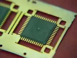
Getting that chip connected to the outside world is another modern marvel and one that is often best served by photoetching the metal contact device. The lattice of conductive material, often copper, to which the semiconductor die is bonded is called a leadframe. The leadframe delivers dozens of interconnect points to the die. The physical connections are made by automated wire bonding machines.
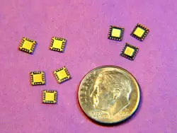
Leadframes are typically made from metal less than .010” thick and may have features that are no wider than the material thickness. Photo etching is the only practical solution to produce parts that are free of burrs and distortions.
These devices can range from simple DIP to very intricate and delicate high density QFN. They are often made from a high performance copper alloy such as C194.
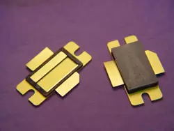
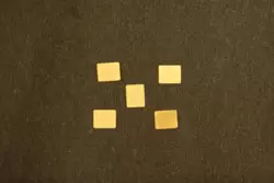
A group of nickel-iron-cobalt alloys, known generally as “glass-to-metal sealing” alloys—of which Kovar may be the best known brand name, are also popular choices for both leadframes and “lids,” the closure devices for hermetically sealed packages. Lids may be flat or stepped and are typically produced without tabs. Again, precision metal etching is the best way to produce parts that are flat and burr-free.