Industry Leaders
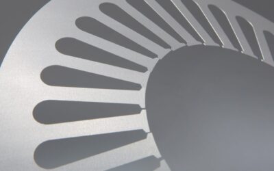
 Conard Corporation has the industry leading process for etching aluminum, developed by the company’s founder, a metallurgist. Other etching companies have Conard do their aluminum etching.
Industries Served
- Aerospace
- RF/Microwave
- Semiconductors + Microelectronics
- Medical Scientific
- Instrument Controls
- Sensors + Mems
- Power Generation + Storage
- Filtration
Photochemical machining is used to produce metal components for many types of aerospace applications from airframe stiffeners and heat sinks to satellite batteries.
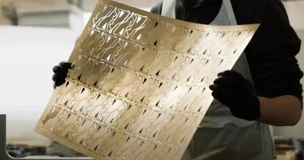
The ability to produce complex parts that are free of burrs and thermal or mechanical distortion in very thin gauges of metal is a key advantage of chemical etching. Precision etched components enable the creation of complex geometries at negligible incremental cost.
Many aerospace components are produced in aluminum to save weight. Photo-etching aluminum is challenging because it is a very reactive metal that readily oxidizes.
Learn MorePhotochemical etching is an economical and productive solution for the many varieties of thin gauge metal parts used for the ever-growing applications in wireless communications. From handsets and Bluetooth devices, to WiFi and Wimax, and cellular tower and satellite components, the ability of precision metal etching to create the complex metal geometries often required offers both speed and cost savings compared to alternative fabrication methods.
Learn MoreMicroelectronics make the world go ‘round. There’s not much left that doesn’t have a semiconductor chip of some sort in it. The semiconductor chip itself is something of modern miracle. The current generation of CPU chips is packing in excess of two billion transistors onto a die about 1-inch square.
Getting that chip connected to the outside world is another modern marvel and one that is often best served by photoetching the metal contact device. The lattice of conductive material, often copper, to which the semiconductor die is bonded is called a leadframe. The leadframe delivers dozens of interconnect points to the die. The physical connections are made by automated wire bonding machines.
Learn MorePhoto etching finds a wide variety of applications in medical devices and systems. Although implantable devices, such as stents, are etched in titanium, etched stainless steel alloys are used extensively in external products.
Stainless steel alloys are preferred for medical applications for a number of reasons including durability, sanitariness, and comparatively low cost. Stainless steel can be sanitized with harsh chemicals or subjected to steam cleaning or an autoclave without damage. Photochemical machining is a preferred method for fabricating many types of blades, closures, filters, sensors, and instruments for both medical and veterinary uses.
Learn MoreEtched Components for Medical, Scientific and Industrial Devices
Some of the varied applications for photo etched metal components include:
- Control and measurement of fluids and gases
- Air and water analysis
- Photonics and optics
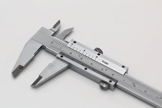
- Metrology
- Spectroscopy and spectrometry
- Chromatography
- Ultrasound and audiometry
- Magnetic resonance imaging
- Precision balances and strain gauges
- Lasers and infrared
- Biomedical sensors and analyzers
- Power and energy measurement and control
Metal Sensors and MEMS Utilize Chemical Etching
Photo etching is an effective solution for producing precision parts that are used in sensing, detecting and measuring applications. These types of components interact mechanically with “the outside world” and electrically with the system or device to which they “report”.
Learn MorePower Generation and Storage Systems
Fuel cells, microturbines and batteries use chemically etched components in a number of ways:
- proton exchange membranes
- fuel plates and flow channels
- heat exchangers
- air bearings
- anode grids
Renewable energy and distributed generation are changing the playing field for electrical power. Solar, wind and hydro power are becoming cost effective compared to commercial generators. Fuel cells and microturbines put power generation where and when it is needed. And, just ask Elon Musk, batteries are about to change the energy storage game again.
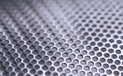
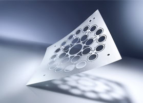
Learn MorePhotochemical etching is an ideal process for perforated metal products, such as:
grids, screens, meshes, filters, separators, microfilters, grilles, lighting diffusers and more
Unlike mechanical perforating methods such as punching, stamping or laser cutting, photochemical machining of metal leaves the material free of burrs and induced mechanical or thermal stress or deformation.
Learn More
How Can We Help?

Conard Corporation has the industry leading process for etching aluminum, developed by the company’s founder, a metallurgist. Other etching companies have Conard do their aluminum etching.
Why Conard?
With 60 years of experience, we are leaders in precision metal manufacturing through photochemical machining in a wide variety of metal alloys. With turnkey services to meet demanding customer requirements, we provide engineering and design support with rapid turn around of prototypes. We also engage in special development projects for customers with complex needs.
Photo Etching Fact
The photo chemical etching process–also known as photo etching, chemical etching, and photo chemical machining– enables the easy production of delicate or complex part geometries reliably and consistently. A wide variety of alloys can be photo etched including nickel, molybdenum, silver, and Kovar, as well as stainless, carbon and silicon steels and most copper alloys.
