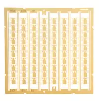
Photo etching is the ideal solution for QFN and LD-MOS leadframes as well as a wide range of custom platforms.
QFN or “air-cavity” packages are widely used in RF and microwave communications applications due to the low attenuation loss. These leadframes are typically very complex and delicate designs that are well suited to the capabilities of chemical etching.
Flat and step lids for hermetically sealed electronics packages are also readily produced by photochemical etching. Common alloys for these applications are often in the nickel-iron family and include Kovar, Invar, F-15, and others.

Many electrically “noisy” products emit interference which must be contained by metal shielding in copper, beryllium copper, brass and others.
Chemical etching is a fast and economical means of producing both simple and complex enclosures and barriers to electromagnetic and radio frequency emissions.
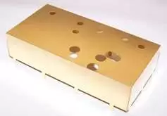
Pictured is an example of an etched and formed enclosure for electronic assemblies.
Direct Bond Copper is another popular application for photo etching. A layer of copper is vacuum bonded onto an alumina ceramic base and a circuit is etched into the copper. Etched DBC parts are used in many RF/microwave applications including cell phones, wireless and and microwave transmitters.

This link leads to the machine-readable files that are made available in response to the federal Transparency in Coverage Rule and includes negotiated service rates and out-of-network allowed amounts between health plans and healthcare providers. The machine readable files are formatted to allow researchers, regulators, and application developers to more easily access and analyze data.